1. Project Overview
Project Background
This project was developed in collaboration with a leading regional public transportation operator and a national smart city system integrator. The transit authority serves over 500,000 daily passengers and aimed to modernize its bus fare collection system.
The original system relied on outdated cash-based payments and limited single-card solutions, which resulted in inefficiencies, longer boarding times, and limited flexibility for passengers.
The goal of this project was to design and deploy a smart, scalable, and industrial-grade payment solution capable of supporting modern digital payment methods and future smart city integration.
Project Goals
-
Automate fare collection to eliminate manual cash handling and reduce labor costs
-
Support multiple payment methods, including NFC, QR code, and EMV cards
-
Improve operational efficiency through real-time transaction processing
-
Enable seamless integration with existing transit and smart city systems
-
Build a scalable architecture for future expansion
Core Challenges
-
Integrating multiple payment interfaces while ensuring stability and security
-
Operating reliably in harsh environments (vibration, -20°C to 60°C temperature range)
-
Supporting offline transactions in areas with weak network coverage
-
Achieving low-latency, real-time transaction processing to avoid passenger delays
2. Client Requirements Analysis
The solution was designed based on strict B2B requirements from transportation operators and system integrators.
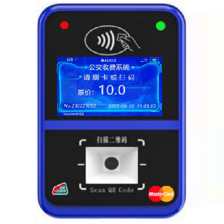
Payment Method Support
-
NFC Contactless Payment
Supports ISO 14443A/B standards, including bank cards, transit cards, and mobile wallets
-
QR Code Payment
Supports dynamic and static QR codes, including integration with mobile payment platforms
-
EMV Card Support (Optional)
Ensures compatibility with global banking and financial standards
Network Connectivity
-
4G/LTE Module for real-time communication
-
WiFi Fallback to ensure continuous connectivity
Industrial-Grade Durability
-
Wide Temperature Range: -20°C to 60°C
-
Vibration Resistance: ISO-compliant testing for vehicle environments
-
IP65 Protection: Dustproof and splash-resistant design
System Functional Requirements
-
Transaction processing within 300ms
-
Offline transaction caching with automatic synchronization
-
Remote device management via cloud platform
-
Real-time monitoring and fault diagnostics
Customization Requirements
-
Custom UI aligned with client branding
-
Multi-language support
-
Logo and interface customization
-
Flexible configuration for different operational scenarios
3. System Architecture
The solution is designed with a four-layer modular architecture, ensuring scalability and maintainability.
3.1 Hardware Layer
-
Custom main control board (core system)
-
NFC module for contactless payments
-
QR scanning module
-
4G communication module
-
Power management system
3.2 Firmware Layer
-
Device control and peripheral integration
-
Secure communication handling
-
Payment data encryption
-
Hardware abstraction and driver management
3.3 Application Layer
-
Payment logic and transaction processing
-
User interface and interaction
-
Driver-side system interaction
3.4 Cloud Backend
-
Transaction processing and storage
-
Data analytics and reporting
-
Remote device management
-
OTA firmware updates
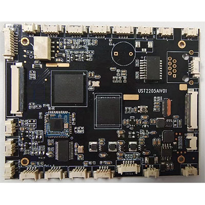
4. Core Board Design
The core board serves as the central processing unit of the entire system.
CPU / SoC Selection
-
Industrial-grade ARM Cortex-A53 quad-core processor
-
Clock speed up to 1.8GHz
-
Optimized for low power consumption and high stability
Interface Design
-
UART ×3
-
I2C ×2
-
SPI ×1
-
USB 3.0 ×2
Supports flexible expansion and integration with peripherals.
Module Integration
-
Pre-integrated NFC, QR, and 4G modules
-
Modular architecture for easy maintenance and replacement
Power Management
-
Wide voltage input (12V–24V)
-
Overvoltage and short-circuit protection
-
High-efficiency power conversion (>95%)
Industrial Reliability
-
Industrial-grade components (-40°C to 85°C)
-
EMI-resistant PCB design
-
Extensive reliability testing (thermal, vibration, aging)
5. Development Process
The project follows a structured embedded hardware development workflow:
-
Requirement Analysis
-
Hardware Design
-
PCB Layout & Fabrication
-
Firmware Development
-
Integration Testing
-
Pilot Deployment
-
Mass Production
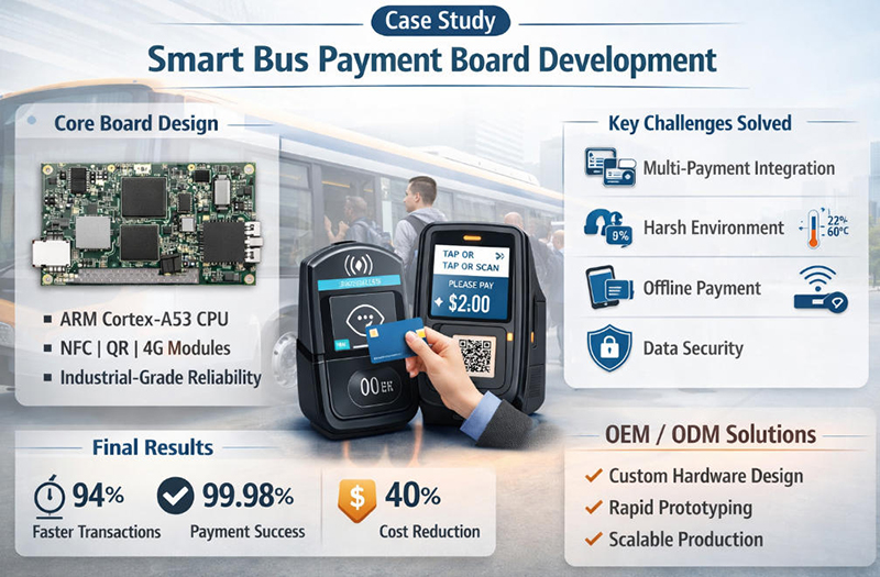
6. Key Technical Challenges & Solutions
Challenge 1: Multi-Payment Integration
Solution:
A unified firmware protocol was developed to standardize communication across NFC, QR, and EMV modules.
Challenge 2: Harsh Operating Environment
Solution:
Industrial-grade components, reinforced PCB design, and IP65 protection were implemented.
Challenge 3: Offline Payment
Solution:
-
Local storage for up to 10,000 transactions
-
Automatic synchronization when network is restored
Challenge 4: Payment Security
Solution:
-
AES-256 encryption
-
Secure Element (SE) integration
-
Secure boot mechanism
7. Final Results
Operational Improvements
-
94% reduction in transaction time
-
40% reduction in labor costs
-
65% reduction in maintenance costs
System Performance
-
99.98% payment success rate
-
Stable operation for over 6 months
-
Remote management of 200+ devices
Scalability
-
Supports up to 1,000 buses
-
Modular expansion for future features
8. OEM / ODM Customization Value
No In-House R&D Required
Clients can launch products without building hardware teams.
Faster Time to Market
-
Prototype delivery: ~60 days
-
Production readiness: ~90 days
Flexible Customization
-
Hardware customization
-
Firmware customization
-
UI and branding customization
Scalable Manufacturing
-
Supports small batch and mass production
-
No MOQ for early-stage prototypes
Cost Efficiency
-
Up to 60% reduction in R&D cost
-
Reduced production and iteration costs
“We provide ready-to-integrate core boards that enable companies to build their own smart bus payment systems efficiently.”
9. Why Choose Us
We specialize in custom embedded hardware development for smart terminals, with strengths including:
-
Advanced embedded system design capability
-
Full-stack development (hardware + firmware + system integration)
-
Industrial-grade reliability engineering
-
Flexible OEM/ODM customization
-
Proven experience in smart transportation systems
10. Conclusion
This project demonstrates how a custom smart bus payment core board can transform traditional fare collection systems into a modern, efficient, and scalable solution.
By combining:
-
Embedded hardware design
-
Secure payment integration
-
Industrial-grade engineering
we help clients build reliable and future-ready smart transportation systems.
11. Call to Action
Looking to develop your own smart payment terminal or embedded hardware solution?
👉 Contact us for custom embedded board development
👉 Get a tailored smart payment solution for your industry
👉 Build your next-generation smart device with us